- Home
- News Release
- 2021
- Commercialization of Pre-cut Anisotropic Conductive Film (ACF)
Commercialization of Pre-cut Anisotropic Conductive Film (ACF), Suitable for Mounting of Camera Modules and Other Components
-ACF Pre-cut to Fit Unique Pad Layouts, Enabling High-density Mounting and Higher Manufacturing Efficiency-
Product
2021.12.13
Dexerials Corporation (Headquarters: Shimotsuke-shi, Tochigi; Representative Director and President: Yoshihisa Shinya; hereinafter, "Dexerials"), which provides leading-edge technologies, materials, and devices for smartphones, automotives, and other products, announced that it has developed and commercialized Pre-cut Anisotropic Conductive Film (ACF), which can be mounted efficiently even when pads layout are designed in a unique form.
This product is suitable for use for pad connection in camera modules and various sensor modules where pads are not arranged linearly. It has been already used for mobile IT devices.
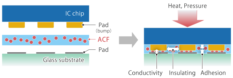
Our Anisotropic Conductive Film (ACF) is a film-type adhesive material that provides three functions: adhesion, the connection of opposite pads, and insulation from adjacent pads. ACF is used for IC chip mounting on flat panel displays. In recent years, its use has been expanded to pad connections of camera modules, touch panels, sensor modules.
■ Illustration of the use of Anisotropic Conductive Film (ACF)
■ Illustration of Camera Module mounting by ACF
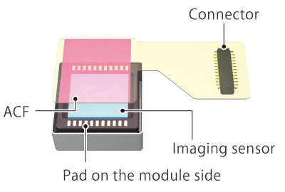
Pre-cut Anisotropic Conductive Film (ACF) as a solution against issues on high-density components mounting of mobile IT devices, etc.
Smartphones and other mobile IT devices are growing more multifunctional. Many components, such as multiple cameras, depth sensors, and a face recognition module, which has resulted in a higher density of components. The efficient use of space is necessary for mounting the large number of components on a circuit board and connecting the pads. There are several ideas for this purpose include arranging pads in a square layout and in two rows (upper and lower rows), instead of the conventional linear layout.
Further, the use of the conventional linear ACF on such a component with a non-linear pad arrangement can be problem. Bonding large-sized ACF to cover the entire surface results in heat and pressure applied to parts other than the pads, which may damage the component. On the other hand, if thin ACF are used only for parts that need it in line with the pad layout, their angle and position need to be changed multiple times. This had been an issue in customers' manufacturing efficiency.
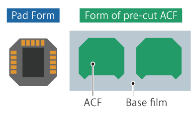
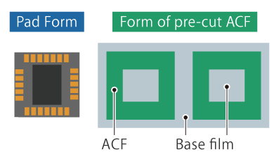
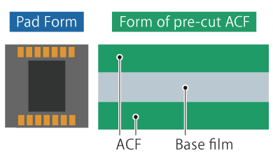
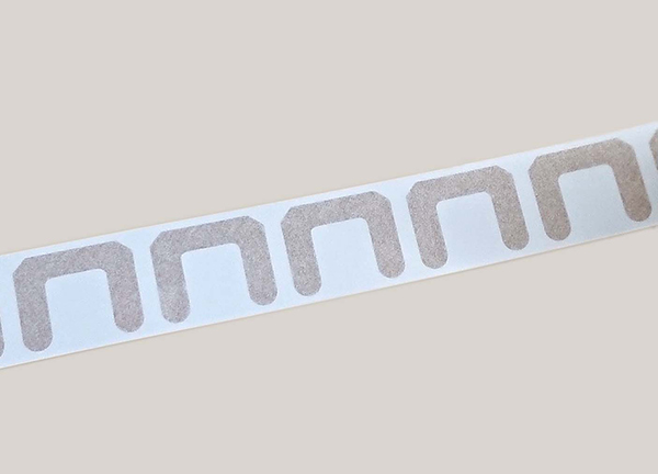
The pre-cut Anisotropic Conductive Film (ACF) developed by Dexerials resolve this issue. The film is pre-cut into independent pieces, hollow squares or rectangular forms, with two rows of ACF and a space in between. It enables efficient mounting of pads with unique layouts.
■ Conventional Anisotropic Conductive Film (ACF)
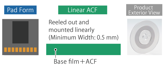
■ Pre-cut Anisotropic Conductive Film (ACF)
Dexerials, which has the world's largest market share*1 for ACF for displays, has successfully commercialized this product by developing a technology for pre-cutting the film into the same forms continuously and accurately, with knowledge on ACF and technologies on adhesion that the company has cultivated for a long time. In addition, the precisely controlled pre-cutting process enables ACF to be pre-cut to be 0.5 mm wide at a minimum. This gives design flexibility in the form of components to mount it on and even higher density mounting, thus contributing to increasing and improving functions of devices.
Details of Pre-cut Anisotropic Conductive Film (ACF)
■ Product Name
- Pre-cut Anisotropic Conductive Film (ACF)
■ Features
- Efficient mounting enabled by pre-cutting ACF for the pad layout or form of the circuit board
ACF is pre-cut to fit the unique pad layouts of various modules, for which high-density mounting is required. It can be mounted in diverse forms, enabling efficient mounting with minimum damage to the component.
- It can be pre-cut to be 0.5 mm wide at a minimum, enabling the connection of pads with the fine layout.
This product can be pre-cut to be 0.5 mm wide at a minimum. This is equal to the minimum slit width of the current conventional ACF (linear ACF), enabling circuit connections in tight space.
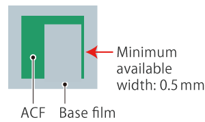
- Center-punching of the ACF into a hollow square/rectangular form is also possible.
It can also be pre-cut into independent pieces with no ACF around each, hollow squares or rectangular forms created by center-punching ACF, and two rows of ACF with a space in between. ACF can be pre-cut into any form to fit the customer's component or use of ACF. This gives design flexibility in the form of components to mount it on and even higher-density mounting, thus contributing to increasing and improving equipment functions.
■ Specifications
| Product | This Product | Our Conventional Product (For Camera Modules) |
|
|---|---|---|---|
| Form | Suitable form based on the customer's design and requirements | Linear (tape Form) | |
| Connection Material | FPC, PCB, Glass, Ceramic Circuit Board | ||
| Minimum Space [µm] *2 | 100 | ||
| Minimum Connection Area [µm2] *3 | 80,000 | ||
| Thickness [µm] | 25 | ||
| Conductive Particles | Type | Gold / nickel-plated Resin Particles | |
| Particle Diameter [µmФ] | 20 | ||
| Main Bonding Conditions | Temperature [℃] | 130 or above | |
| Time [sec] | 6 or more | ||
| Pressure [MPa] *4 | 0.5 or above | ||
Demand for fine connections is expected to rise with increasing opportunities to use sensor modules, reflecting the digitalization of society, the expansion of IoT, and the development of autonomous driving, which will lead to increases and advances in the functions of applications. Dexerials will continue to improve its knowledge and technologies on ACF cultivated over many years, which have resulted in the world's largest market share*1 for ACF for displays and other achievements, thus providing products and solutions that support digital technologies.
- *1 The 2020 share for value amount of ACF for large-sized and small to medium-sized displays according to the “Reality and Future Prospect of Display Related Market 2021” issued by Fuji Chimera Research Institute,inc.
- *2 Minimum space: Space between adjacent pads
- *3 Please contact us for information on σ value control of the minimum connective area for each product individually.
- *4 Pressure of main bonding: The pressure at COG bonding is described as the total area of bumps. The pressure at FOG, FOB and FOF bonding is described as the bonding area.


