- Home
- News Release
- 2006
- A new ACF batch bonding connection method with relevant developed material put into practical use
A new "ACF batch bonding connection method" with relevant developed material put into practical application
New Product
2006.08.03
Sony Chemical & Information Device Corporation (hereafter referred to as Sony Chemical & Information Device) has developed a new method to allow simultaneous bonding of multiple chips using ACF (Anisotropic Conductive Film), which was thought to be difficult to implement, and a specially designed ACF to accommodate the newly developed mounting method. The new ACF-based packaging process and the specialty ACF could potentially lead to a quantum leap in productivity with an excellent quality.
Background of the new packaging technique development
Sony Chemical & Information Device Corporation has been challenging in semiconductor Flip Chip packaging industry from application-oriented (customized process) to simple general-purpose.
In 1996, Sony Chemical & Information Device Corporation (previously Sony Chemicals Corporation) put the world's first ACF for CSP (Chip Size Package) on the market. Since then, ACF has been the subject of widespread attention for its various advantages such as available batch packaging of multiple leads, achievable fine pitch designs and possible reduction in size and weight, and research and development have been focusing on the applicability to the packaging process. At present, ACF is highly regarded for its capability of bonding at electrode pitches of even less than 50μm and it has been adopted in some semiconductor packaging applications involving control and/or memory chips and in package production based on Flip Chip bonding with ACF.
However, ACF is not applicable as a routine approach in the semiconductor package market due to the lower productivity in the bonding of chip. Existing ACF-based semiconductor packaging requires pressure application to chips and the substrate to be kept free from any inclination and bonding requires precise adjustment of individual chips. In addition, packaging of a single chip takes about 20 seconds for bonding and curing, which gives rise to the problem that many different pieces of equipment are necessary to increase production output. The newly developed technique with special ACF resolves the issues and broadens the range of ACF-based packaging methods in the semiconductor packaging market.。
Features of the new packaging method and specialty ACF
1: Simultaneous pressure application to multiple chips, contributing to significantly reduction of the bonding time per chip to several tenths
The biggest advantage of the new method developed by Sony Chemical & Information Device is the reduction of the bonding time per chip to several tenths and thus significantly increased productivity of the packaging process. The new method allows simultaneous multiple chips bonding and bonding of several tens of chips at the same time which have been pre-bonded on a combination board by installation of a newly developed special tool to existing thermo-compression bonding equipment. The batch bonding of 40 chips in 20 seconds, for example, results in a significantly improved production tact time of 0.5 seconds or less per chip if ACF processing time should be divided per chip which gives a great contribution to reducing production lead time.
2: Substantial increase in productivity without any great investment。
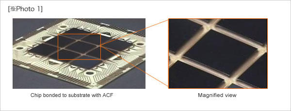
The second advantage is negating the need for huge sums of investment in facilities and equipment since development does not require any complicated equipment. For development of ACF bonding involving multiple chips simultaneously, many attempts have been made though there is no practically applicable method established to date since the simultaneous bonding of multiple chips by existing bonding equipment fails to achieve proper flatness of individual chips. The new method developed by Sony Chemical & Information Device resolves this problem and allows uniform and accurate pressure application and mounting for all chips involved based on a simpler mechanism. This eliminates the need for flatness adjustment requiring greater accuracy and ensures a substantial increase in productivity. [※Photo 1]
3: Elimination of minute voids, ensuring higher reliability of packages
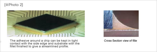
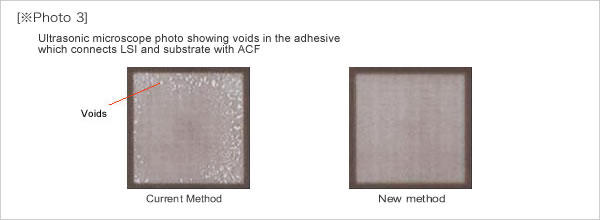
The new method, when applied in combination with the concurrently developed specialty ACF, eliminates minute voids between chips and substrate that cannot be removed using existing methods, thus ensuring remarkable enhancement of package reliability. In addition, the resin around the circumference of chips called fillet [※Photo 2] can also be finished to give a streamlined profile without involving any voids [※Photo 3], which constitutes an additional advantage for its reliability.
4: RoHS Directive-compliant, environmentally conscious method
The package for semiconductor based on the ACF bonding are free from any lead content and then, the new development makes it easy to ensure compliance with the RoHS Directive and is also safe, with no environmental impact. Sony Chemical & Information Device believes that the newly developed method and specialty ACF would be widely adopted as a multi-chip mounting method for semiconductor packaging technology using ACF for its high potential to dramatically increase productivity in semiconductor packaging.
-ACF batch bonding connection method -