- Home
- News Release
- 2004
- Double-sided flexible printed circuit board developed to support high-density mounting The NMBI technology-bas
Double-sided flexible printed circuit board developed to support high-density mounting The NMBI technology-based double-sided flexible circuit board to get into volume production
New Product
2004.12.06
Sony Chemicals Corporation has completed the development of double-sided flexible printed wiring boards adopting the NMBI (Neo Manhattan Bump Interconnection) technology, the layer-to-layer interconnection on a printed wiring board. The company is starting sample shipments in the spring of 2005 and production in the summer.
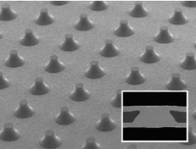
The NMBI technology features the fundamental building blocks: a manufacturing process for formation of copper bumps (projections) on a substrate by etching and a processing method for intra-layer electrical interconnections between the etched copper bumps and the copperwhich is hot-pressed onto the bumps. Sony Chemicals has been conducting engineering development to commercially introduce the printed wiring boards adopting this technology under a licensing agreement signed December 2002 with North Corporation, the inventor of the fundamental building blocks of this technology. As a result, Sony Chemicals has successfully realized the ultra-low profile boards to enable high-speed transmission and high-density mounting by adopting this technology to double-sided flexible printed wiring boards. The developed boards allow finer pattern circuitry, higher component packaging density due to the Pad on Via (*1), and improved electrical characteristics due to the copper-to-copper metal interconnection.
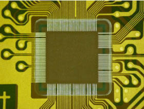
Presently, Sony Chemicals has succeeded in developing original manufacturing techniques for volume production of printed wiring boards to ensure consistent pressure for interconnection of bumps, enhance the accuracy in circuitry pattern, and ensure compatibility between peel (bending and tensile) strengths and connection reliability. The design rules for the double-sided flexible printed wiring boards subject to the volume production schedule consist of a set of a 65µm pitch wiring pattern, a land diameter of 250µm, and a bump pitch of either 0.35 mm or 0.30 mm. We at Sony Chemicals are pioneering double-sided flexible printed wiring boards in the industry for high-density mounting, which could reduce the board area by approx. 41% compared to conventional through-hole connection.
Our double-sided flexible printed wiring boards allow further downsizing, slimming down and/or weight reduction of cellular phones, PDAs, digital still cameras, video cameras, PCs and other mobile devices when applied in the peripherals for LCD or camera module in the devices. The double-sided flexible printed wiring boards are to be adopted for the displays of Sony's mobile devices. The boards will be also marketed outside of Sony Group.
Application of our manufacturing techniques will be expanded to FPC (flexible printed circuit) for COF (*2), high-speed transmission flat cables, module boards, and package for semiconductor. We continue to make continual improvements aiming at finer wiring patterns, higher density mounting and increased number of layers.
*1 Pad on Via: Allows higher density mounting as a component could be mounted directly above interconnects between layers (etched bump).
*2 FPC for COF: Flexible printed wiring board to support fine-pitch, high-density mounting, accommodating the bare chip mounting of semiconductors

SEM photograph of etched bumps on copper foil/Cross-section of double-sided board showing an interconnect via (etched Cu bump) (Inset at the lower right)

Double-sided flexible printed circuitwiring board for COF with a wiring pattern pitch of 65µm
The contents of this article are current at the time of publication.
Please note that this product has been discontinued and we are no longer accepting orders or providing samples.

